


How to Use a Laser Engraver for PCB and Component Labeling
I run a small electronics design studio — three engineers, mostly power electronics and motor control boards. For the first four years, we outsourced PCB labeling. Every board revision meant a turnaround wait and a minimum order. When I finally put a fiber laser in the back of our shop, the first thing we ran was a batch of 30 development boards — each one needed a unique serial number, a revision mark, and our company logo. The whole batch took about 40 minutes. We had the boards the same day we made them. I should have done it four years earlier.

Laser engraving PCB boards and electronic components covers a wider range of applications than most makers and electronics shops realize. It goes well beyond the industrial semiconductor marking covered in manufacturing literature — it includes hobbyist DIY PCB fabrication, professional board labeling, R&D prototype marking, and small-run production identification for contract electronics manufacturers. This guide covers the practical how-to: what laser type works for what PCB application, how to set up LightBurn for board labeling, common pitfalls, and real workflow examples from electronics shops and makers.
What Is PCB Laser Engraving and What Can It Do?

According to Wikipedia's printed circuit board overview, PCBs are used in virtually all electronic products to mechanically support and electrically connect components. Laser engraving on PCBs creates permanent marks on the board surface — date codes, serial numbers, revision marks, component labels, QR codes, and company logos — through a non-contact process that doesn't stress the board or its components.
There are two fundamentally different contexts for laser engraving PCBs. The first is fabrication — using a laser to actually remove copper to create circuit traces, which is a technically demanding and equipment-intensive process primarily used in professional and R&D environments. The second — and far more common — is labeling and marking: adding permanent text, codes, and identification to finished or partially assembled boards. This guide focuses on labeling and marking, which is accessible to makers, small shops, and production electronics companies alike.
|
PCB LASER APPLICATION |
EQUIPMENT REQUIRED |
WHO USES IT |
|
Board labeling (serial, date, logo) |
Fiber or CO2 laser |
Makers, small shops, contract assemblers, production |
|
Component identification marks |
UV or fiber laser |
Electronics manufacturers, EMS companies |
|
Silkscreen text replacement |
Fiber or CO2 (FR4) |
Prototypers, small-run production |
|
QR / 2D codes for traceability |
UV or fiber laser |
Contract manufacturers, production lines |
|
Prototype PCB fabrication (trace etching) |
High-power diode or CO2 + chemistry |
Advanced makers, R&D departments |
|
Depaneling (board separation) |
UV laser (preferred) / CO2 |
EMS companies, flex PCB manufacturers |
🛠️ REAL MAKER EXPERIENCE
Tom runs a small IoT device company — six employees, about 400–600 board builds per year. Before the fiber laser, every production run needed a paper label stuck to each board for traceability. Labels shifted, fell off in assembly, and occasionally ended up on the wrong board. After adding a 30W fiber galvo laser, he laser-marks each board with a serial number and 2D code before any assembly happens. The marks survive hand soldering, wave soldering, and cleaning. 'I haven't had a traceability gap in two years,' he says. 'And the boards just look more professional to customers when they open the enclosure.
Which Laser Type Works for PCB Labeling?

Fiber Laser for Metal Housings and Dark Board Surfaces
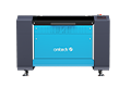
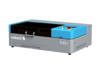
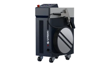
Fiber lasers at 1,064nm are absorbed by metals and work well on PCBs that have dark soldermask surfaces — the laser creates high-contrast marks through ablation or color change on the soldermask coating. Standard FR4 boards with green, black, or dark blue soldermask can be effectively labeled with a fiber laser at appropriate power settings. OMTech's fiber laser engraving machines with galvo scanning heads are the production standard for batch serial number marking on boards with dark soldermask.
CO2 Laser for FR4 Boards and Cutting
CO2 lasers at 10,600nm are absorbed by the organic materials in FR4 substrates, making them useful for marking the board material itself on bare or light-colored FR4, and for cutting PCBs. OMTech's CO2 laser engraver machines can cut FR4 PCBs cleanly at appropriate power settings, and some makers use CO2 lasers with LightBurn to create prototype circuit board layouts by exposing the PCB to ferric chloride etchant after laser ablation of a resist coating — an accessible DIY approach that doesn't require wet chemistry for the resist application step.
UV Laser for Professional PCB Marking (Production Grade)
UV lasers (355nm) produce the highest quality PCB markings for professional production environments: minimal heat-affected zone, solder-resistant marks, and the ability to mark assembled boards without risking thermal damage to placed components. UV laser marks on FR4 survive the full reflow soldering process and aqueous cleaning. For production electronics companies marking boards before assembly, UV laser is the professional standard — though the equipment cost is higher than fiber or CO2 systems.
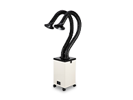
⚠️ IMPORTANT: CO2 LASER AND PCB SAFETYFR4 (the most common PCB substrate) contains epoxy resin, fiberglass, and brominated flame retardants. When cut or engraved with a CO2 laser, it produces toxic fumes including hydrogen cyanide and brominated compounds. Always use proper fume extraction rated for electronics materials when laser engraving or cutting FR4. Never mark or cut PCBs in an enclosed space without air filtration. Some EMS and PCB manufacturers specifically prohibit CO2 laser cutting of FR4 due to fume management requirements — UV laser cutting is the cleanroom-compatible alternative. |
Step-by-Step: PCB Labeling Workflow with a Fiber Laser and LightBurn

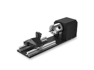
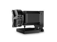
The most common practical PCB laser engraving application for electronics shops is batch serial number and date code labeling on dark soldermask boards. Here's the workflow for OMTech's galvo fiber systems with LightBurn, which handles variable data and database-connected serial sequences directly. OMTech's Galvo Fiber Laser Marker collection includes systems compatible with LightBurn variable text for this exact application.
|
1 |
Export your board outline from KiCad or EagleCAD as SVG or DXFExport the board outline layer (Edge.Cuts in KiCad) and your desired marking area as a vector file. Mark the center point of your intended label area — this becomes the alignment reference in LightBurn. Vector formats ensure your text and marks scale accurately without pixelation artifacts. |
|
2 |
Import into LightBurn and set up variable textImport your board outline as a reference layer (set to no-cut, visible only). Create a new layer for your label text. Use LightBurn's variable text feature to set up a serial number sequence: Tools > Variable Text > Serial Number. Set your start number, prefix, and suffix format. For batch labeling, set the increment to automatically advance with each job. |
|
3 |
Calibrate laser parameters for your soldermask colorBlack soldermask typically requires 15–25% power at 300–500mm/s for a clean fiber laser ablation mark. Green soldermask requires slightly different parameters — start a test on scrap board material from the same batch before running production. The goal is high-contrast marks with no charring or surface damage to adjacent copper areas. |
|
4 |
Set up a board fixture for repeatable alignmentConsistent fixture positioning is the key to batch labeling without manual repositioning between boards. A simple jig of scrap acrylic cut to the board footprint works well for low-volume runs. For higher volumes, a multi-board fixture plate allows marking 4–8 boards per job setup. Confirm the first board's mark position before running the full batch. |
|
5 |
Run the first board and verifyMark one board and verify mark position, contrast, and character legibility before running the full batch. Use a USB magnifier or loupe for fine character sizes under 2mm. Scan any 2D barcodes or QR codes with a barcode reader app to confirm readability before batch production. |
|
6 |
Run batch with variable text auto-incrementWith LightBurn variable text active, each subsequent job automatically increments the serial number. Place the next board in the fixture and press start — no re-entering data between boards. For a batch of 50 boards with a single serial number field and a logo, typical cycle time is 15–45 seconds per board depending on content complexity. |
Common PCB Laser Engraving Applications in More Detail
Date Codes and Revision Marks
Every production electronics board benefits from a date code — typically year and work week — and a hardware revision mark. These permanent laser marks allow field service teams and quality engineers to identify exactly when and at what revision a board was manufactured without relying on documentation that may not travel with the board. For small electronics companies, this is often the first laser marking application they implement and the one that demonstrates the most immediate operational value.
Company Logo and Branding on Development Boards
Electronics product startups and custom hardware developers use laser branding on development and evaluation boards as a professional presentation element. A logo on a dev board handed to a potential customer or investor communicates attention to detail that a bare PCB doesn't. The laser mark is permanent across years of testing and field use — the board's brand identity doesn't peel or fade regardless of handling.
2D Data Matrix Codes for Production Traceability
For electronics manufacturers producing boards for sale or contract assembly, laser-marked 2D codes linked to production records are increasingly required by customers. The 2D code connects each physical board to its assembly records, test results, component lot traceability, and quality inspection data. A fiber laser marks a scannable 2D code on a bare PCB in 2–5 seconds — fast enough to be incorporated inline in most assembly workflows without becoming a production bottleneck.

Component Value Labels and Assembly Guides
For complex boards assembled by hand — particularly in R&D and prototype environments — laser-marked component labels adjacent to pads reduce assembly errors. Reference designators and component values marked directly on the board eliminate the need to constantly reference assembly drawings. This is also useful for boards assembled by contract manufacturers unfamiliar with the design — clear permanent marking reduces rework from component placement errors.
OMTech Systems for PCB Labeling
Here are two OMTech fiber systems well-suited for electronics board labeling:
|
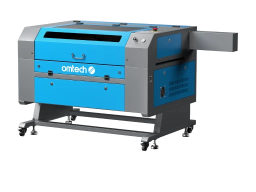
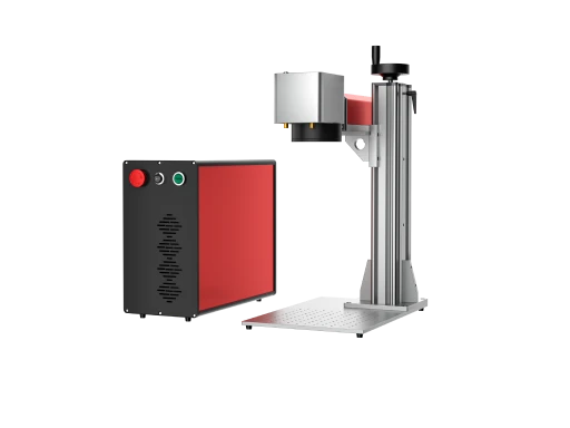
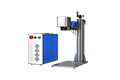
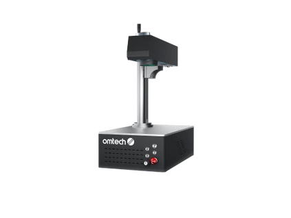
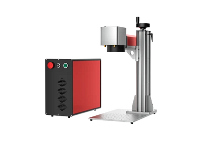
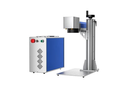
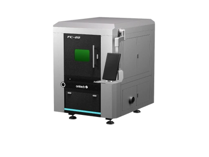
Galvo Fiber 20/30/50W — PCB Serial Numbers • Batch Labeling • 2D Codes Galvo scanning head for fast batch PCB labeling. Compatible with LightBurn variable text for auto-incrementing serial number sequences. Autofocus handles board thickness variation. Handles dark soldermask (black, green, blue) boards with high-contrast ablation marks. Used by electronics startups, contract assemblers, and IoT hardware companies for board-level traceability, date coding, revision marking, and company logo placement on production boards. |
|
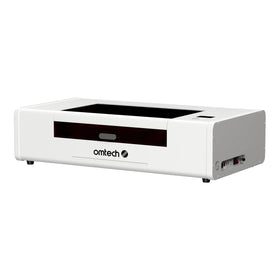
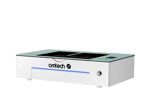
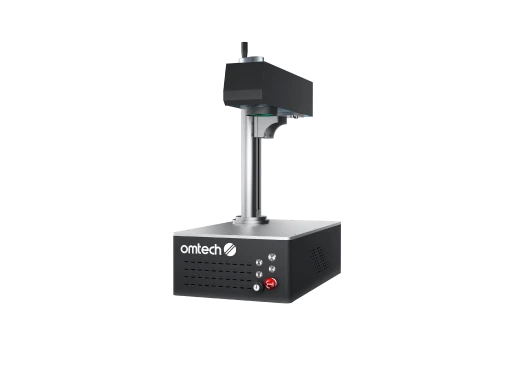
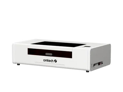
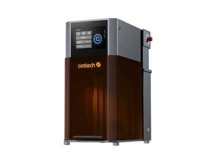
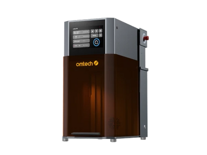
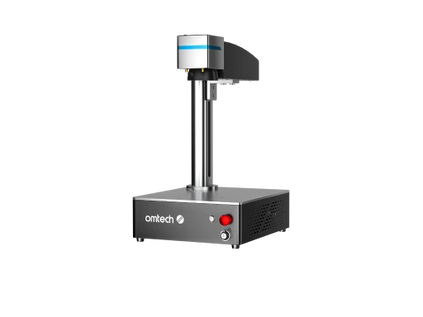
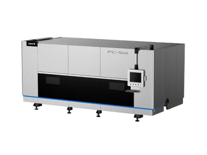
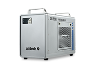
Galvo Fiber 30W Integrated Marker — Compact Footprint • Small Boards • Dev Labs 30W integrated galvo fiber system with compact 5.9" × 5.9" work area. Used by electronics labs, R&D departments, and small electronics shops for development board labeling, prototype marking, and small-batch production board identification. The compact integrated design requires minimal bench space — useful in electronics labs where workspace is shared with test equipment and assembly stations. EzCad variable data support for serial number batch production. |
|
💡 FOR METAL PCB ENCLOSURES AND HOUSING LABELS Electronics products sold to customers require identification on the product enclosure as well as the board. OMTech's MOPA fiber laser engraving machines handle aluminum and anodized enclosures, panel labels, and product identification marks on metal electronics housings. OMTech's professional laser setup support is available for electronics shops setting up both board-level and housing-level marking workflows. |
Ready to add laser marking to your PCB production workflow? |
Frequently Asked Questions
What is PCB laser engraving?
PCB laser engraving (also called PCB laser marking) is the process of using a focused laser beam to permanently mark printed circuit boards with text, logos, barcodes, serial numbers, and other identification. The laser creates a permanent mark on the board's soldermask, substrate, or copper surface without mechanical contact. It is used for date coding, batch and serial number traceability, revision marking, component labeling, and company branding on production and prototype boards.
Which laser is best for marking PCBs?
For batch production labeling on dark soldermask boards (black, green, dark blue), a fiber laser with a galvo scanning head is the practical choice — it's fast, works well on soldermask surfaces, and integrates with LightBurn variable text for serial number automation. For assembled boards where thermal damage to placed components is a concern, a UV laser produces solder-resistant marks with minimal heat impact. CO2 lasers can mark FR4 but require excellent fume extraction due to toxic off-gassing from the substrate material.
Can a laser engraver make PCBs from scratch?
A laser engraver can be used in PCB fabrication, but the process is complex and not comparable to professional fabrication. The most practical DIY approach uses a laser to ablate a resist coating on a copper-clad board, which is then etched with ferric chloride to remove exposed copper and create circuit traces. CO2 and high-power diode lasers are used for this. The resulting boards have trace widths and spacing limitations compared to professional photolithography-based PCB fabrication, but they're useful for rapid single-layer prototype work.
What LightBurn settings work for PCB labeling?
For fiber laser marking on black soldermask FR4 boards, typical starting parameters are 15–25% power, 300–500mm/s speed, and 20kHz frequency for a 30W galvo fiber system. Green soldermask requires slightly higher power — start at 20–30% and test on scrap material from the same batch. LightBurn's variable text feature (Tools > Variable Text > Serial Number) enables auto-incrementing serial numbers across batch runs. Export your board outline from KiCad or EagleCAD as SVG or DXF for use as a positioning reference in LightBurn.
What information should be laser marked on a PCB?
Standard PCB laser marking content includes: date code (year and work week, e.g., '2025-W14'), hardware revision (e.g., 'Rev 2.1'), manufacturer or product logo, serial number (for production traceability), and optionally a 2D Data Matrix code linking to production records. Compliance marks (CE, FCC, RoHS) are also commonly added. For internal development boards, adding the designer's initials or project name helps track which board version is which during multi-revision R&D programs.
Can you laser engrave an assembled PCB with components on it?
Yes, with appropriate laser selection and placement. Fiber laser marking on the soldermask surface of an assembled board is practical if the marking area is on bare soldermask away from components. UV laser marking is preferred for assembled boards in professional environments because of its minimal thermal impact. Avoid marking directly over or adjacent to heat-sensitive components (oscillator packages, MEMS sensors, large capacitors). Always test on an unpopulated board first and confirm that no thermal damage occurs to nearby components before running production.
How small can text be on a laser-marked PCB?
Fiber laser systems with galvo scanning heads routinely mark readable text at 1.5mm character height on PCB soldermask surfaces. With careful power and speed calibration, characters down to 0.8–1mm height are achievable on high-contrast soldermask (black soldermask gives the best contrast with fiber laser ablation). For QR code and Data Matrix marks on boards, a 5mm × 5mm code is a practical minimum for reliable scanner readability. Smaller marks require lower power, slower speed, and finer focus settings — always verify readability with an actual barcode scanner before batch production.
Does laser marking affect PCB solderability or electrical performance?
Properly applied fiber laser marks on soldermask surfaces do not affect the solderability of exposed pads or the electrical performance of nearby traces. The soldermask coating in the marked area maintains its protective properties. Marks should not be applied directly over solder pads, copper traces, or through-hole pads. If boards undergo aqueous cleaning after soldering, fiber laser marks on soldermask are resistant to the cleaning chemistry and maintain legibility. UV laser marks specifically are solder-resistant and are commonly applied before the reflow soldering step.
What are common mistakes when laser engraving PCBs?
The most common mistakes are: using too much power (causing charring or soldermask delamination beyond the mark area), marking over copper pads or traces (damaging the pad coating), using CO2 laser on assembled boards without adequate fume extraction (toxic fumes), not testing parameters on scrap material before production runs, and using raster image files instead of vectors (poor mark quality at small sizes). Start with conservative power settings (10–15% for a 30W fiber) and increase gradually until you achieve the contrast you need without surface damage.